
[ad_1]
We have talked several times about perovskite and its natural ability to interact with light, a characteristic that has made it extremely attractive in the field of photovoltaics, alongside silicon in tandem solar cells.
This strategy has made it possible to mitigate the weak points of the perovskite and to reach – and overcome – 30% efficiency in the conversion of solar radiation into electrical energy.
Excellent results that have pushed the search even further, reaching the point of searching ways to take silicon out of the equation and exploit only perovskitemuch more abundant in nature and easily workable, as well as naturally flexible and semi-transparent.
An international engineering team, with members from from three different Universities (University of Toronto, Northwestern University and University of Toledo)have joined forces and created a monolithic tandem solar cell using only perovskites. The result is a perovskite mono block in which the different solar units are made to grow on top of each other. The team of researchers employed two different layers of perovskites, each tuned to a different part of the solar spectrum; the study was published by natures.
“In our tandem solar cell, the top layer of perovskite has a wider bandgap, which absorbs ultraviolet and some visible light well”explains Chongwen Li, researcher and co-author of the publication. “The bottom layer has a narrow bandgap, which is tuned more towards the infrared part of the spectrum. Between the two, we cover more of the solar spectrum than would be possible with silicon.”.
The trump card of the new module is though the inverter, inserted in a new and very thin coating between the perovskite and the electron transport layer. The material has improved it displacement of charges by inhibiting the recombination between electrons and their respective holes.
The team’s prototype produced an open circuit voltage of 2.19 electron voltsa record for all-perovskite tandem solar cells, achieving a conversion efficiency of 27.4%although the independent certification of the National Renewable Energy Laboratory in Colorado, recorded a 26.3%.

Perovskite is being joined – successfully – also to the graphene, a two-dimensional material with boundless potential.
In fact, it is located in Heraklion, the capital of Crete a solar park where they are experiencing the most advanced photovoltaic panels in the world, composed of perovskite and graphene, developed and manufactured entirely in Italyby the researchers of the University of Rome Tor Vergata, of the startup BeDimensional SpAGreatcell Solar Italia, the Italian Institute of Technology (IIT), the Institute of Structure of Matter of the National Research Council (CNR-ISM) and the University of Siena, together with the Hellenic University of the Mediterranean.
“The work stems from a community project that began in October 2013 involving researchers and scientists from every country. Ten years of basic research on graphene and a one billion euro budget have made it possible to build the foundations for the many industrial applications of today. And ours is one of the fields of use, precisely the photovoltaic one”explained Francesco Bonaccorso, co-founder and scientific director of the startup Bedimensional.
With a output power greater than 250Wsimilar to the one that can be generated with 60 crystalline silicon cells assembled in a 160 x 90 cm panel, according to the technicians produce 1 kWh of electricity from this optimized solar park has an environmental footprint of around 50% less compared to using the electricity mixes currently used in Europe.
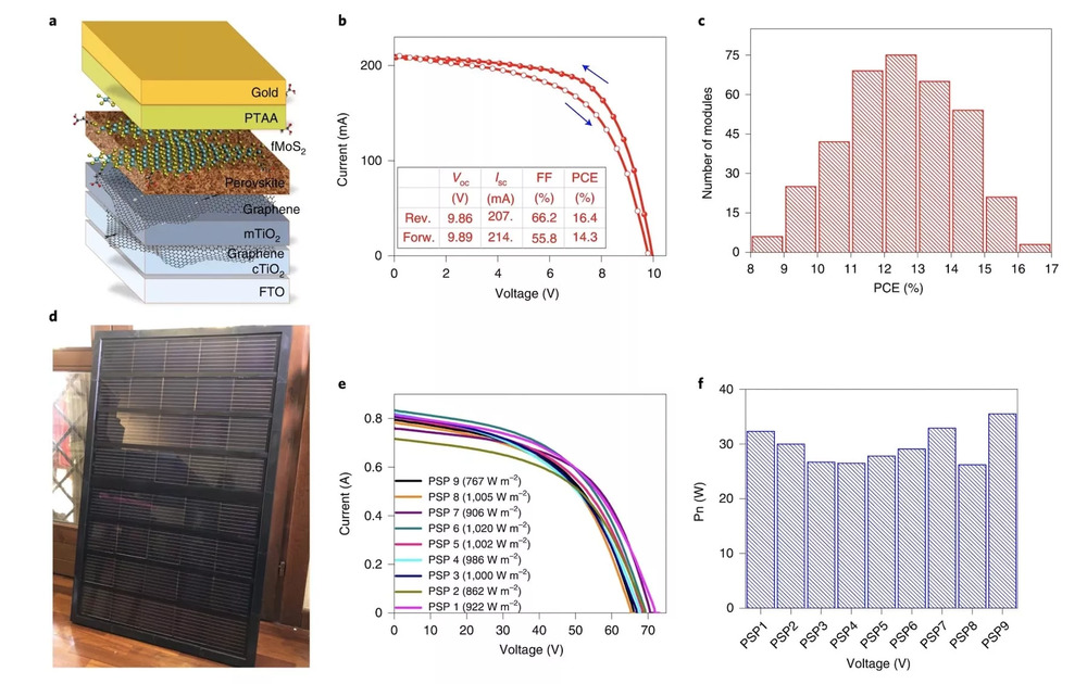
The experimentation of the Cretan solar park is not finished yet, as, according to the experts, there is still great room for improvement in efficiency, currently around 18%.
Here you can read and download the study.
.
[ad_2]
Source link